Carbon nanotube processors have hit a vital milestone in computing history. MIT researchers built a modern microprocessor that contains more than 14,000 carbon nanotube field-effect transistors (CNFETs). This achievement shows a most important step forward in this promising technology. Carbon nanotube transistors are a big deal as it means that they deliver 10 times better energy efficiency and faster speeds than silicon alternatives.
Over the last several years, we’ve tracked carbon nanotube technology progress and its scaling challenges. The latest breakthrough comes from new techniques like DREAM. This innovation lowered the carbon nanotube purity requirements from an impossible 99.999999% to a more realistic 99.99%. Peking University’s researchers took this further and created the world’s first carbon nanotube-based tensor processing unit for AI processing. Their unit achieved remarkable energy efficiency beyond 1 TOPS/w while using only 295μW of power. The team’s RV16XNano processor, which uses RISC-V architecture, ran a modified version of the classic “Hello, World!” program. This proves that carbon nanotube computers have moved beyond theory into reality.
Why Silicon is Reaching Its Limits in Modern Chips
Silicon-based computer chip industry now faces major physical barriers that slow down state-of-the-art and efficiency gains. The search for alternatives like carbon nanotube processors becomes crucial as we reach the basic limits of silicon technology.
Moore’s Law Slowdown and Energy Inefficiency
The historical pattern of doubling transistor density every two years broke when silicon scaling slowed down dramatically since 2016. Intel needed five years to move from 14nm to 10nm technology instead of the expected two years. Computational energy could match global energy production within 30 years at current rates. Data centers use about 2% of all electricity in the United States, which shows an emerging energy crisis in computing.
Manufacturing advanced chips has become extremely expensive. Quantum effects interfere with reliable operation as transistors shrink to atomic scales—the smallest commercially available being just 3 nanometers wide. Manufacturers hit a clock rate ceiling since 2004, and they had to adopt multi-core designs that don’t automatically improve performance for many algorithms.
Thermal Constraints in 2D Silicon Architectures
Heat management stands as a critical barrier in silicon technology. Modern chips create substantial thermal energy that becomes harder to dissipate as devices get smaller and more powerful. Electronic devices have grown thinner (from 25mm to less than 10mm) while their power consumption has more than doubled (from 3W to 7W).
The thermal challenges in 2D architectures include:
- Increasing package power density without proportional increases in heat dissipation capacity
- Thermal cross-talk between components requiring isolation
- Limited thermal conductivity of interposer materials
- Heat spreading constraints within thinning form factors
Systems often throttle performance to prevent overheating due to this thermal bottleneck. Heat can cause premature aging in circuits, data loss in memory, and mechanical stress from disparate expansion between materials.
These basic limitations in silicon technology explain why researchers actively study carbon nanotube processors as a promising alternative with better energy efficiency and thermal characteristics.
Breakthrough Techniques in Carbon Nanotube Chip Fabrication
Manufacturing defects have blocked carbon nanotube processor development’s path to success. We have a long way to go, but we can build on this progress through three innovative techniques that have helped overcome these challenges.
DREAM: Designing Resiliency Against Metallic CNTs
DREAM technique marks a breakthrough for carbon nanotube technology. CNFETs needed semiconducting purity of about 99.999999% to work correctly—a level that seemed impossible. DREAM places metallic CNFETs in strategic positions to prevent interference with data processing. This approach relaxes the strict purity requirement by about four orders of magnitude (10,000 times) to a more achievable 99.99%.
Custom software identifies logic gate combinations that can withstand metallic CNTs and those that remain strong despite their presence. The software automatically picks only resilient combinations during chip design. MIT researcher Shulaker explained that manufacturers can “buy carbon nanotubes off the shelf, drop them onto a wafer, and just build circuits like normal”.
RINSE: Selective Exfoliation to Remove CNT Bundles
RINSE process tackles another major hurdle—carbon nanotube bundles that form during deposition. These bundles act as with tangled spaghetti and create particle contamination that disrupts circuit function.
RINSE process has three key steps:
- Wafer’s pretreatment with an adhesion agent
- Polydimethyldiglutarimide (PMGI) polymer coating
- Solvent sonication to remove polymer and bundles
This method reduces particle density by more than 250 times compared to other approaches. Single carbon nanotubes stay firmly attached to the wafer’s surface.
MIXED: Metal Interface Engineering for P/N CNFETs
Digital computing needs both P-type and N-type transistors, which don’t deal very well with carbon nanotubes consistently. MIXED technique fine-tunes CNFETs for specific functions through precise engineering.
Different metals attach to each transistor—platinum for P-type and titanium for N-type transistors. Oxide compounds coat CNFETs through atomic-layer deposition. This process lets researchers adjust transistor characteristics for specific applications. The approach will give consistent performance across thousands of transistors and enables complex processor designs.
These three techniques have paved the way for the first commercial-grade carbon nanotube processors. They solve manufacturing challenges that once limited this technology to theoretical research.
Demonstration of the First Commercial Carbon Nanotube Processor
Carbon nanotube computing has jumped from theoretical concepts to ground reality with a working processor. MIT scientists teamed up with Analog Devices to build a groundbreaking device that shows this technology’s commercial potential.
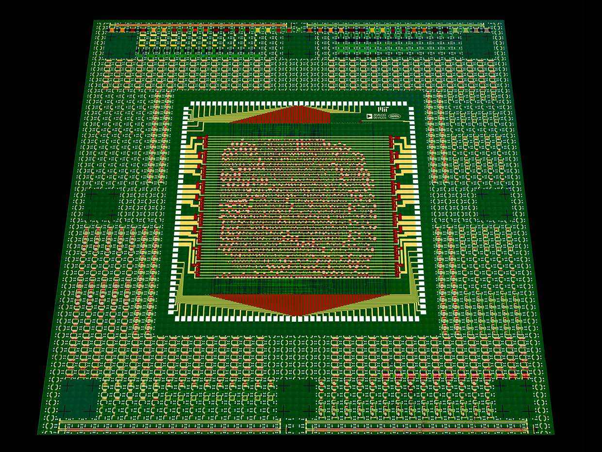
RV16XNano: 16-bit RISC-V Processor with 14,000 CNFETs
Scientists revealed the RV16XNano in 2019, a remarkable achievement that packs roughly 14,000 carbon nanotube field-effect transistors (CNFETs). This 16-bit microprocessor runs on the open-source RISC-V instruction set architecture and works smoothly with existing software development tools. The processor handles 32-bit instructions through 16-bit memory addressing. This marks a huge step forward for carbon nanotube computing. Professor Max Shulaker stated, “This is by far the most advanced chip made from any emerging nanotechnology that is promising for high-performance and energy-efficient computing”.
Execution of Full Instruction Set and Hello World Program
The RV16XNano ran the complete RISC-V instruction set successfully. This proved its ability to match a conventional microprocessor’s functions, though at slower speeds for now. The team put it through the classic programming test: a modified “Hello World” program. The processor passed with flying colors, outputting: “Hello, World! I am RV16XNano, made from CNTs”. This confirmed its status as a fully working computer.
Comparison with Previous 1-bit CNT Prototype
Stanford University built the first carbon nanotube computer, Cedric, back in 2013. That early prototype had just 178 transistors, crawled at 1 KHz, and could only process single bits of information. The RV16XNano leaves these numbers in the dust with an 80-fold increase in transistor count and much broader capabilities. This shows how far the technology has come over six years.
The current processor’s 1.5-micrometer size matches Intel’s silicon-based 80386 processor from 1985. We have a long way to go, but we can build on this progress before reaching modern silicon performance levels.
Path to Commercialization and Industry Integration
Carbon nanotube processors stand out because they work well with today’s silicon manufacturing setup. This compatibility could speed up their adoption by semiconductor companies.
Manufacturing in Silicon Foundries Using Standard Equipment
Carbon nanotube processors don’t need special equipment like other new technologies. They can be made using regular silicon-chip manufacturing methods. Two commercial facilities have already shown success in making CNT transistors: Analog Devices’ silicon plant and SkyWater Technology’s foundry. These places used their regular equipment to produce carbon nanotube transistors on standard 200-millimeter wafers.
The team’s new deposition method marks a breakthrough. The original process took 48 hours, but they made it faster through advanced techniques like dry cycling. This method sticks CNTs to the surface by taking out and drying the silicon wafer regularly. Now it takes just 150 seconds. This speed improvement by 1,100 times solves a vital problem for commercial production.
DARPA and Analog Devices Collaboration
A $61 million DARPA project has given strong support to make this technology commercial. MIT researchers teamed up with industry experts at Analog Devices and SkyWater Technology for this initiative.
SkyWater’s president Thomas Sonderman shared his view: “We are excited to continue our work building out the critical infrastructure for enabling commercial market availability of CNFETs. This effort is a pivotal move to bring back manufacturing of leading-edge advanced computing to the U.S.”.
Professor Max Shulaker explained why this partnership matters: “Bridging the gap between lab and industry is something that researchers ‘don’t often get a chance to do,’ but it’s an important litmus test for emerging technologies”.
Projected Timeline for Market-Ready CNT Chips
Shulaker feels optimistic about the future: “We think it’s no longer a question of if, but when”. His team believes we could see commercial carbon nanotube chips in stores in less than five years.
The carbon nanotube market keeps growing. Experts predict it will expand from $150 million in 2019/2020 to more than $500 million this decade. As the technology gets better, it can work alongside existing silicon chips.
Carbon nanotube transistors might first complement silicon rather than replace it, especially in 3D chip stacking. Shulaker adds: “The process that the team has developed is almost at room temperature, so we can build layers of CNT transistors directly on top of an existing CMOS chip”.
Conclusion
The Dawn of Carbon Nanotube Computing
Carbon nanotube processors mark a turning point in computing history. The breakthrough achievements highlighted in this piece show how theoretical possibilities have transformed into commercial reality. Research teams have finally conquered the biggest hurdles through innovative techniques like DREAM, RINSE, and MIXED.
Silicon-based computing now faces clear physical limits. Moore’s Law has lost momentum, energy efficiency has hit a ceiling, and thermal constraints hold back performance gains. Carbon nanotube processors represent more than just an improvement – they are the next step in computing architecture.
The RV16XNano processor’s creation, featuring 14,000 carbon nanotube transistors, proves this technology works. While it matches 1980s silicon processors, this milestone sets a clear path forward. The processor runs a complete RISC-V instruction set and executes a “Hello World” program, which verifies years of theoretical work.
Carbon nanotube technology provides a practical upgrade path rather than forcing a complete overhaul. Manufacturers can use existing silicon foundry equipment to produce these processors, which removes major adoption hurdles. Through collaboration with industry partners like Analog Devices and DARPA funding support, the path to commercialization grows stronger.
Market-ready carbon nanotube chips could arrive in less than five years. These transistors will enhance silicon in specific applications before they potentially take over broader uses. The technology works well with 3D chip stacking, which opens up new design possibilities beyond silicon’s limits.
Carbon nanotube processors could solve both performance and energy challenges that threaten computing’s future. Current limitations aside, the core benefits – 10x better energy efficiency and faster speeds than silicon – make this technology a frontrunner for next-generation computing. Silicon won’t disappear overnight, but carbon nanotubes have proven they can lead us forward.
Leave a Reply